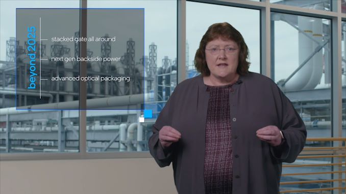
AnandTech Interview with Dr. Ann Kelleher: EVP and GM of Intel’s Technology Development
[ad_1]
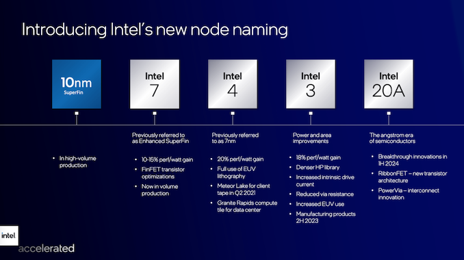
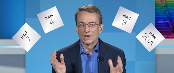
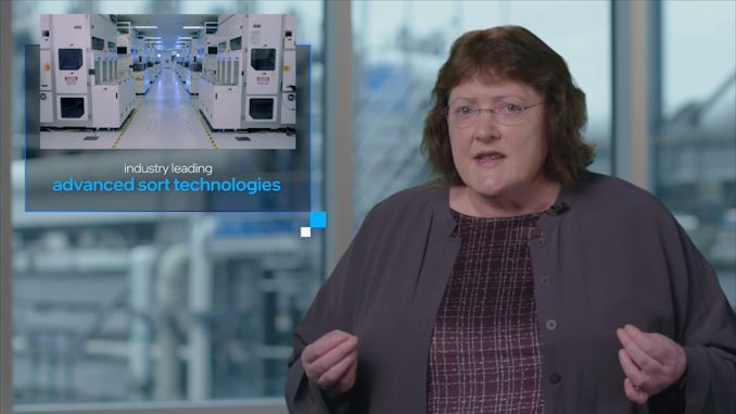
It’s somewhat of an understatement to say that Intel’s future roadmap on its process node development is one of the most aggressive in the history of semiconductor design. The company is promising to pump out process nodes quicker than we’ve ever seen, despite having gone through a recent development struggle. Even with CEO Pat Gelsinger promising more than ever before, it’s up to Intel’s Technology Development (TD) team to pick up the ball and run with it in innovative ways to make that happen. In charge of it all is Dr. Ann Kelleher, EVP and GM of Intel’s Technology Development, and on the back of some strong announcements last year we reached out for the chance to interview her regarding Intel’s strategy.
Dr. Kelleher is a long-time Intel employee, going back 26 years and starting in Intel Ireland. Starting with semiconductor research, Dr. Kelleher took roles in manufacturing, rising through the ranks to Fab Manager and then being in charge of all of Intel’s manufacturing facilities. The pivot to Technology Development, as we’ll see in the questions below, is a complementary move that brings together both the experience of development and manufacturing. What I loved about speaking to Ann is the element of quiet but striking determinism in the way she spoke – for as much as the CEO is shouting from the rooftops about Intel’s ability to execute, a few minutes with Ann showcases just how focused the people who have to do the research and development really are and how important it is to them on a personal level.
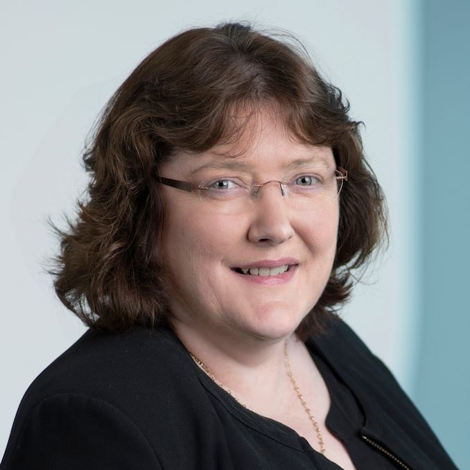 Dr. Ann Kelleher Intel | 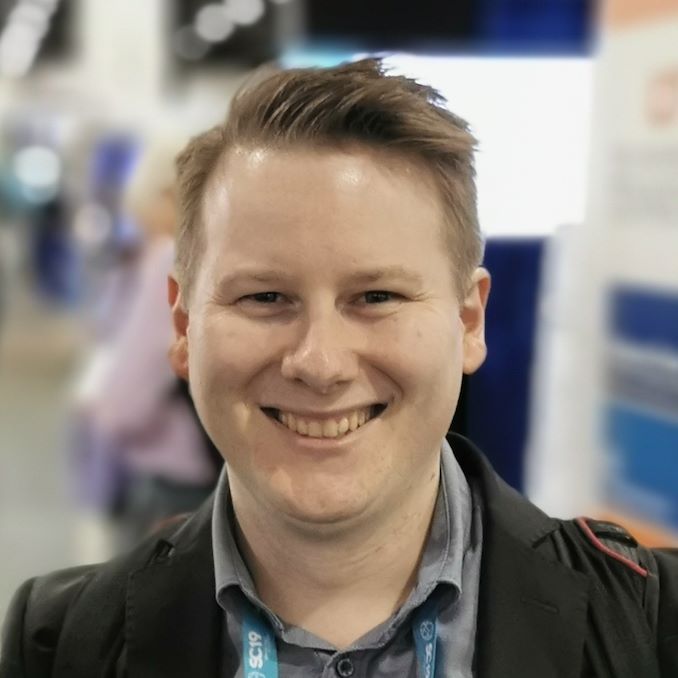 Dr. Ian Cutress AnandTech |
This interview took place before Intel’s Investor Meeting.
Ian Cutress: Going through your history, you joined Intel in early 1996, making you a 26-year veteran of the company – an Intel ‘lifer’! In working up from Process Engineer, to now GM of Technology Development, what exactly has been your journey through Intel?
Ann Kelleher: Well, I started back in 1996 – maybe I even started a little bit before 1996. When I was in college, I did a Master’s and a PhD – I did it in a research centre in Ireland, which was called the National Microelectronics Research Centre, which was in Cork. Then when I finished there, I went to imec in Belgium and I did a postdoc, and then I returned to Ireland. Then I was leading a small research group, in the same research institute as my PhD, but Intel Ireland was starting up a factory at the time. It was a new factory that became Fab 14. They were hiring for Fab 14, and at the time they basically asked me to come and talk to them, they asked me to come and interview, and I did.
I got the job. At the time, I thought I would come for a year. A lot of my job prior to joining Intel was basically writing project proposals so that I would have enough money in research to fund the group that I was leading. One of the challenges in [writing those proposals] was that I always had to write down what my industrial experience was, and at the time I hadn’t worked in the industry. So I would always try and explain all the projects I’d done within the industry. So when Intel Ireland offered me the job, I thought I’d go work at Intel Ireland and industry for a year or two, and I’ll tick that box, and then I’ll go back to research. But I found that when I joined Intel Ireland, and when I joined Intel overall, the pace of Intel was much faster than the pace of that in research, and it allowed me so much opportunity from a career perspective, from a growth perspective, from a learning perspective, from a job change perspective, that it basically really suited me.
I will say over the last 26 years, Intel’s been really good to me. Now I’ve done very well, I’ve worked very hard, I’ve delivered a lot, but I think we were a match. So instead of staying 2 years, I’ve been with Intel for 26.
IC: After starting at Intel as a process engineer, and moving into Fab management, what experiences from managing the fab side of things translate into becoming the Executive Vice President in charge of how Intel’s future process nodes will work?
AK: I came into the manufacturing world from a research development background, and then when I came into it, I worked as a process engineer first. I then became a group leader, then I became a department manager, and then I became a factory manager. Then I moved from Ireland to the United States, and I was a plant manager in Arizona. Then I became a site manager in New Mexico, then I became head of the Fab, basically a co-head of all the Fabs, and then I co-headed TMG (Technology and Manufacturing Group). So I was in manufacturing again, but now I’m in Technology Development.
A lot of my time and my journey within Intel, within the manufacturing organization, was that I did a lot of technology transfers. These are technology transfers from Technology Development into the factories. So my life with Intel over the 26 years started in Ireland, and I’ve spent time in California, Phoenix, New Mexico, and Oregon. So a lot of my time over the years was spent such that when I wasn’t working directly on development, I was closely working with the technology development organization, bringing the technologies into manufacturing.
Now, when you’re bringing in, and starting up the technology, in manufacturing, you have to learn a lot about the technology itself. You have to learn a lot about it, how it was made, and how you can set it up so you can ensure that it runs with success. Within that journey, I became very appreciative of the work that the Technology Development organization needed to do. I also became very appreciative of the work that the manufacturing organization needed to do, so that you could get the best of both worlds. So then when I came over to TD, I brought in my skills and my learning from the manufacturing side, and I brought my past learning in terms of all those technology transfers – the time that I spent as what we call ‘SEED’ within the technology development organization. I will say from my life pre-Intel, I brought a deep appreciation for the technical skills. I would say Intel has many of the leading engineers and scientists within the world, so it gave me a chance to bring my experience together so that we get the best of both worlds.
IC: How would you characterize Intel’s Technology Development Team compared to the traditional R&D that we hear about?
AK: Within the technology R&D, we focus on process development and packaging development. The overall R&D umbrella at Intel captures many aspects of R&D: there is circuit design, and there are our labs – and I know you’ve done a past interview with our labs! There’s all of that aspect, but the aspect that we cover in R&D is process development: where the silicon wafers are processed, we develop the next generation technology that gets used in our next-generation products. Equally well, we do packaging development, and that is development of the next generation type of packaging for our products. So between the combination of our next-generation technology and packaging, we’re able to deliver our future products. I view the process and technology, as the heart at Intel, because if we do our job really well, we deliver not just the present, but we’re also making the future. I tell my team that we need to deliver really well the present, but we’re also making the future.
IC: So when we traditionally speak to Intel about future development, they talk products that are coming up in 1-3 years as being very ‘immediate’, then we have research to 5 years out, and pathfinding at 7+ years away. Can you kind of talk about how much mental space each of those take up?
AK: I think it varies in any given week. It also varies in any given 6 months, right? I mean, let’s be honest – when I came over to TD, my entire first 6 months was on process. I gave a little bit of time to the rest, but I was really focused on process development. But within the last 6 months, going into 2022, I’m spending a lot more time focusing on what we call ‘components research’ for our future. Me and my team had a very extensive set of publications at IEDM in December, for example. But one of the things we do in components research is all about the innovations that are enabling us to move the frontier of Moore’s Law. That is absolutely critical. It is absolutely valued by me, and in 2022, a lot of my attention will be in that space.
IC: Semiconductor development has often been quoted as the industry whereby you bet the company in every generation, especially when it comes to the leading edge. It’s no secret that CEO Pat Gelsinger is publicly stating that Intel is going to accelerate its process node roll-out: five nodes in four years, which would be the fastest development ever in semiconductor history. Intel by contrast has recently gone through some of its slowest node development in its history, taking a while to get 10nm into a higher yielding profitable situation with acceptable margins. It seems a large task to go from a historical slow to an industry-wide fastest ever track. You’ve been in this position for 18 months – can you speak to what strategic changes you’ve put in place compared to what was done previously? Which of these execute on Pat’s vision? For example, when we last spoke, you mentioned more ‘backup strategies’ are in place!
AK: I’ve done a lot more than when we spoke last! I have been working with the team since I joined, and I break it down into a number of portions.
First of all, I’m very focused on predictable execution. I bring that from my background in manufacturing, and I bring that from my own core – I like getting stuff done, and I like getting stuff done on time! I was like that pre-Intel, and I’m like that at Intel, so it has a lot of focus. So to then get within predictable execution, we have broken it down into many portions.
I spoke to you before about our risk assessment methodology, and we’re looking at where we need to do contingency plans. Then within those contingency plans, we look at what time it would make sense to execute, how long to continue them without deploying, and what is the right time to cut across and move from the primary plan to the contingency plan. We have had that risk assessment scheme in place since August 2020, and that was one of the actions we have had in place if needed on our P1276, our Intel 4 process. That methodology has been working very successfully for us.
Over the years, we’ve done a lot of work with the ecosystem. But now we’ve also started to enhance that work, and we’ve taken it to the next level. I’ll break it down into our equipment vendors, materials vendors, our suppliers, and our EDA (Electronic Design Automation) tool suppliers. We have spent a lot of extra focus in how we make sure we’re learning from the ecosystem – we don’t need to learn everything ourselves, and what is key is that we keep the innovation at Intel in the key places for differentiation. That means we need to get from A to get to B, achieve parity, and get ahead. Then we take what we have learned from within the ecosystem, and build from that. So we have a very active focus on that, and that has been working well for us.
We’ve also been very focused on adopting industry standards. For industry standards, in particular we talk around our process design kits or PDKs, and ensuring they all work with the EDA (Electronic Design Automation) vendors. There are a lot of industry standards out there that we can pick, so we have picked and placed and brought in the ones we need. Now one of the things that we’re doing is bringing those industry standards into Intel, and at the same time, we’re looking where we have the best from our IDM, and how do we combine both of those together.
The other thing, and I say this many, many times, is that I work with some of the best engineers in the world within this organization. I also did some organisational structure management changes over the last 18 months. I would say that we’re more streamlined, and very clear in where we’re going, very clear on the mission, very clear and the deliverables, very clear about the schedule, very clear on where we have the opportunities to do stuff earlier. So there is a lot of focus, I would say.
As well as that, we have that focus on innovation – we’re not going away from that. We’re focused on innovation, discipline around our execution, enabling our risk assessments and contingency planning, getting the best from our equipment vendors, getting the best from our material suppliers, equipment suppliers, and enabling our EDA suppliers. It’s across many fronts. We’ve said ‘here’s what we’re going to do, and we’re doing what we were saying’.
IC: So is this the Gelsinger Era of Intel, or the Kelleher Era of Intel? [laughs]
AK: Pat is our CEO, and Pat has done a wonderful job since he’s joined us. He’s been really, really supportive. I know I said some of this work has started before Pat joined, but one of the key things is that he has been really supportive. Part of the focus is that we built a very detailed roadmap on how we get back to parity and get back to leadership, which we shared last July, but that needed money and funding. Pat was very happy to sign the check.
IC: Pat’s vision of Foundry Services, combined with current semiconductor demand requires a diverse portfolio of nodes, not only at the leading edge, but also more commodity notes. Intel is working on 22FFL and a new 17/16nm node, but we see other foundries offering analog, RF, high voltage, packaging, and other optimizations. How diverse does Intel’s offering need to be, especially across Intel’s global infrastructure?
AK: I’ll start with saying what I’m very focused on, and then about what I view as my key four steps in enabling IFS to be exquisitely successful. I’m very focused on getting to our leading nodes, ensuring we’re at parity then into leadership on our Intel 20A, and then our Intel 18A. I’m also very focused on our 22 FFL and our Intel 16 – we’re very focused on making sure that that’s ready for our foundry customers, as well as our packaging. Beyond that, there are a lot of other items that could be on our docket, could be on our table, but for me, my first port of call, my first deliverable, is to deliver those exquisite and successful nodes. Then when we get beyond that, we can talk about more.
This interview was before Intel’s announcement of the acquisition of Tower Semiconductor for $5.4b.
IC: You mentioned earlier about standardization: using industry standards and then combining that with your PDK. This is to enable something to future IFS customers, but also for use internally. If this is the current direction, why was Intel using so many custom tools inhouse? Also, how has that pivot been to moving from these completely custom tools to something more industry standard that you can promote as an IFS offering?
AK: If I go back over the years, I think this is more a historical answer in terms of why were we doing custom tools. We were an IDM that was servicing internal customer projects, our own design teams, and thereby over that time we had built a suite of tools that worked. We have progressed on one path, but the rest of the world, particularly those with the foundries, needed to establish that standardized set of tools and needed to put those standards in place – they could go from tech node to tech node and actually maintain those standard for their customers. So I think historically we were in different places, and we were servicing internal versus external.
As we pivot over to support our external customers (and we had started this pivot even before Pat had announced the IFS), we had started that pivot because externally there was a very large ecosystem which had developed a very robust set of software. It did not make a lot of sense to continue to try and do that and hit the same point for our own internal suite of tools. So it made a lot of sense to start pivoting over.
Now there are cases where we have some unique tools from our past which are a definite benefit to us, which we have held on to, but they’re in addition to the tools. The pivot started in early to late 2019/early 2020 timeframe. It has been very well received internally by our design teams, because it has set the standard for them in terms of things that are not changing at the rate that they had before. It means there is a very clear standard for which they can work to. The ease of use of design is one of the metrics we looked at, and based on all the work that’s been done in our ease of use, we benchmark internal tools with external tools across the external foundry world, and our ease of use has significantly improved. We believe we’re heading towards the best-in-class for that space.
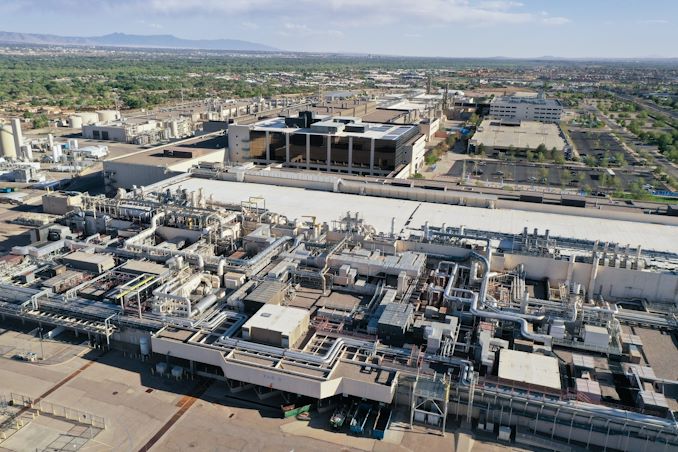
IC: We’re hearing of an internal battle inside Intel when it comes to installing and ramping new process nodes between the different Fabs. It sounds like Leixlip/Laim an Bradoin will be the first for Intel 4 production. How much does TD get involved with the roll-out of new nodes beyond the ‘development’ stage? How cognizant does TD have to be regarding resources and infrastructure for where updated nodes and fabs will be located?
AK: There’s an entire process which goes through, as part of our long-range planning, into the decision on which factory gets the next node. I used to run that when I ran manufacturing, Keyvan Esfarjani does that now because he runs manufacturing. It’s technology development, also technology transfer, to the first HVM (high volume manufacturing), so I need to be, and my team need to be, very cognizant and we work hand-in-hand with the team together to ensure the success of the transfer into the first Fab. We’ve always done that, and we already have very active teams with our Intel 4 – that work is well under progress. So it’s not a case of ‘there you go, good luck!’, I feel ownership, TD feels ownership, until all the factories are completely matched and the transfer is healty.
IC: The development of Intel’s 10nm family of process nodes has been difficult and stretched. The struggles have been noticed, in both product and financials. I know this was before your current role, but could you go into how the development process of 10nm and its challenges provided experience into how Intel might approach similar in the future?
AK: If I go to the highest level, 10 nm was basically attempting and aiming at getting very, very aggressive scaling. I think that in the desire to achieve that very aggressive scaling, EUV wasn’t ready at the time when the 10 nm node was being defined. Had EUV been ready at that particular point in time, I think 10 nm would not have had the challenge that it had. Out of that, we took significant learnings – our risk assessment processes as one. Also when EUV became ready to deploy, it was too late to go back and insert it into 10 nm based on the way the architecture had been designed.
Another key thing we were looking at is building a lot more flexibility in to future process nodes. We’ve overtly said that we will always be on the leading edge of lithography going forward, so we’re designing our process nodes such that if a new piece of leading lithography becomes available and ready, we can cut it in as soon as possible. We don’t want to be in the space where it’s too late to cut it in.
So I think there is that 10nm aggressive scaling that was there, but EUV wasn’t ready, and by the time it was ready, we couldn’t cut it in. So basically we have taken learnings around building in a lot more flexibility in terms of how we set ourselves up for future nodes, and as well as that, the key risk assessments are absolutely critical so that you have that contingency plan ready if you run into problems. We’re trying to land atoms on atoms, or even sometimes half an atom on an atom. So you will have challenges, but the key thing is to have enough options so that the challenge doesn’t get you stuck and slow you down.
IC: As part of that 10nm development process, Intel spoke about scaling boosters and developments such as Contact Over Active Gate (COAG), use of Cobolt and Ruthenium, but never confirmed which ones made it to production or met targets for 10nm. Would you be able to discuss how those have worked, or tweaks made, or other improvements not previously mentioned?
AK: I prefer not to go into the very specifics of a particular process node, but I think out of those you mentioned, a lot of the metals that you’ve mentioned, they continue within the part of the periodic table that we continue to use. Contact Over Active Gate has had its benefits. I think overall, in terms of those areas that give us the real challenge, one or two we have moved away from and others we have kept because we’ve learned how to make them work very, very appropriately in the nodes. As we move onto Intel 4, we didn’t need some of them, because Intel 4 is the first process node where we’re using EUV, and allowed us to streamline our process flow and absolutely eliminated some of the need for those ‘tricks’ that we were using to get to the smaller dimensions.
IC: You’ve actually answered my next question because I was going to ask why Intel relied more on self-aligned quad patterning and other boosters, rather than bringing EUV – but it sounds like the process node, how it was developed, the timing just mismatched.
AK: Yes, and that’s why one of our key learnings going forward. We will have that flexibility going forward, so that if there is a mismatch, that we don’t get caught.
[Ann’s cat, Shadow, makes an appearance in the interview]
IC: When I was in Intel’s D1X Fab (the development fab), I did get to see the EUV machines up close. I touched one and then got told off for it! It was also fun to look inside it as well, because you guys are still installing so many of these machines. When High-NA comes around, if by some reason it’s not ready, or there are other challenges, could I surmise from what you’re saying that for the future nodes that are along those timeframes, if they are ready earlier, the idea is to bring it in earlier? Or if it doesn’t arrive as intended, that there’s flexibility for those layers that may or may not have been High-NA?
AK: Correct. We’re aiming to introduce it in more in 2025, and we’re setting up our processes so that if for some reason High-NA is not ready, then we will be able to continue without it. As soon as High-NA is ready, then we’ll be able to put it into our product and use it.
IC: Intel already has orders in for High-NA machines from ASML. The first-gen NXE:5000 for development, and it’s just been announced that you’ve ordered a second generation NXE:5200. What exactly will you be using the High-NA development machine for?
AK: The NXE:5000 is currently being built for us at ASML. When I visited ASML late last year, I saw the pieces as it was being built and put together. But we’re also working with ASML, and as soon as their first High-NA tool is available for us, we will be running some of our experiments in their lab on that. so that will we will be starting as early possible. So as soon as the NXE:5000 docks, they will be able to cut over and then run it in our own Fab. So we have a very active team working right now with ASML, and those teams are working through all the line items that need to get done, so that by the time the NXE:5000 arrives, that we’re good to go and good to go on the development work in our Fab.
IC: When I’m quoted how long it takes to install an EUV machine and tune it, usually it’s about six months for each, will the first-gen High-NA UV machine be similar or are you trying to improve that?
AK: We’re always striving to drive down the qual (qualification) time. Right now, I’m not in a position to quote what its final qual time will be, but we will be taking as much as possible in learning out of the install quals of the 0.33 NA (regular EUV), basically to apply them to the 0.5 NA (High-NA). There is work to be done, is the simplest way of putting it.
IC: A lot of foundry offerings are built on long-term nodes that form large parts of the market. Other nodes disappear as quickly as they appeared. We’re seeing other offerings at 7nm, 5nm, becoming those long-life nodes. Is there anything different that TD does when it comes to that mind-set of creating a long-life node?
AK: Not really. I will say not really because when we set up our nodes for running within our factories, we’re driving for high yields, we’re driving for really meeting all our criteria, and ensuring that the process node can run at its best. Then when it’s in volume, we continue to run on some performance and enhancement improvements. I think longer-term when the nodes are running within the factories, requests may come from customers that require some unique work or some new unique development work. We would then be supporting that, but it would be very much based on some unique or custom requests from the customers rather than doing anything other than our work that we normally do: continuing to improve yields, continuing to drive down costs, all of the work that we always do. So I think the unique piece would be based on any unique customer asks.
IC: Design Technology Co-Optimization, or DTCO, has been marked by other foundries as the key driver to optimize specific customer products on their leading edge process nodes. The ability to optimize a given design, specifically for performance and power at the transistor level, above and beyond the traditional design kit for a specific layout. Does TD have a plan when it comes to extended DTCO with both its internal development teams and future IFS customers?
AK: Yes, it does. We have a very active program internally on DTCO. That program has been running several years, and it’s been working with our internal design teams. Similar with our IFS customers, TD, and the IFS organization, we will work with customers to ensure that the DTCO happens appropriately for the particular product and the particular requirement of a customer. It’s a key part of the work that we do today.
IC: During 10nm rollout, it was clear that process node development information was hard to come by – Intel didn’t really want to talk about it. Pat often talks about Intel being more ‘open’, whether that’s software, product, or engineering. As Intel moves into that IFS model, how ‘open’ are you expecting Technology Development to be when it comes to major and minor tweaks?
AK: Well, our July event last year is probably the first time we’ve ever been that open in terms of where we are in terms of our roadmap, out as far as 2025. For our customers, we’re fully transparent in terms of our process, we’re fully transparent in terms of our data, and we’re fully transparent in terms of working with our customers to meet their needs. So I think if in this very situation with our customers, were fully transparent, we then at a higher level, we’ve opened up quite a lot too, so I think it’ll be very situational depending on their particular ask.
IC: Pure-play foundry offerings often partner with a fabless semiconductor company to help develop new nodes and packaging offerings. Historically we know that Intel TD works with Intel Product, but for the future, to what extent is TD ready to work with leading edge foundry customers when it comes to next-generation process nodes?
AK: I expect we will be working with both! It could very well be that an external customer is ahead of the internal. That could happen! But equally our internal customers also move on to our new nodes, so I expect that we’ll be working with both, and we have key learnings from both.
IC: We are seeing the leading EDA tool vendors start talking about AI-accelerated offerings when it comes to PDK integration and development. Are there elements of Intel’s process node development that are currently using machine learning, and what are they doing?
AK: We work with the EDA vendors that you’re talking about, and we do work quite a lot in terms of the feedback we do with them, back into the TD organisation, and the process development organization. But if I look across my entire process development organization, we use AI. I mean, it depends on what you want to call it – some people call it machine learning, some people call it advanced analytics, some people call it AI, but we use all of those tools in many areas of our process. We have a lot of process control, which is tied into the equipment process steps, and we feed forward information. We also feed backward information in terms of the previous steps of across the process. We have done a lot of work, and a lot of the benefits in our recent nodes has been because of the use of AI, machine learning, etc. That is a key strand, and one of my groups which reports to me deals with how we continue to move that frontier forward – how we basically apply the best of all the technology, of our own technology, back into our factories.
IC: We’re seeing Intel increase investment into R&D overall; are you seeing some of that in TD, where is it going, and is it enough?
AK: Yes, yes, and yes! I’m seeing increased investment into TD. Is it enough? Yes, for now – I’m sure I’ll always have my hand out for more, right? There’s always more work it can do, but I also need to be pragmatic and realistic. I am spending more money in process development, and I’m spending more on advanced research, and I’m spending more money on package development.
IC: Is there an aspect of Intel’s TD approach that you think is under-promoted to a wider public audience?
AK: I think I could promote some of the work we do in components research a lot more, because that’s the frontier of moving Moore’s Law. I think also over our history, we tended not to talk a lot about it, right? You probably didn’t get to speak to many TD folks over the years, and I think I’m opening that up because I want people to get a visibility into some of the wonderful work that the engineers do.
Many thanks to Ann and her team for their time.
Final thought: Speaking with Dr. Kelleher was great, and I’m sure I could have spent another couple of hours asking for finer detail! With any luck, Intel will have regular manufacturing and technology development update events to detail how the roadmap is progressing. I’m hoping with the disclosures Intel is making on its development progress, as well as the willingness to have interviews with press like me, will lead to a new era of openness from Intel on its manufacturing technology and portfolio.
[ad_2]
Source link

